- 您现在的位置:买卖IC网 > Sheet目录337 > LH28F008SCHT-TE (Sharp Microelectronics)IC FLASH 8MBIT 85NS 40TSOP
�� �
�
�LHF08CTE�
�12�
�4.1� Read� Array� Command�
�Upon� initial� device� power-up� and� after� exit� from� deep�
�power-down� mode,� the� device� defaults� to� read� array�
�mode.� This� operation� is� also� initiated� by� writing� the�
�Read� Array� command.� The� device� remains� enabled�
�for� reads� until� another� command� is� written.� Once� the�
�internal� WSM� has� started� a� block� erase,� byte� write� or�
�lock-bit� configuration,� the� device� will� not� recognize�
�the� Read� Array� command� until� the� WSM� completes�
�its� operation� unless� the� WSM� is� suspended� via� an�
�Erase� Suspend� or� Byte� Write� Suspend� command.�
�The� Read� Array� command� functions� independently� of�
�the� V� PP� voltage� and� RP#� can� be� V� IH� or� V� HH� .�
�4.3� Read� Status� Register� Command�
�The� status� register� may� be� read� to� determine� when� a�
�block� erase,� byte� write,� or� lock-bit� configuration� is�
�complete� and� whether� the� operation� completed�
�successfully.� It� may� be� read� at� any� time� by� writing� the�
�Read� Status� Register� command.� After� writing� this�
�command,� all� subsequent� read� operations� output�
�data� from� the� status� register� until� another� valid�
�command� is� written.� The� status� register� contents� are�
�latched� on� the� falling� edge� of� OE#� or� CE#,� whichever�
�occurs.� OE#� or� CE#� must� toggle� to� V� IH� before� further�
�reads� to� update� the� status� register� latch.� The� Read�
�Status� Register� command� functions� independently� of�
�the� V� PP� voltage.� RP#� can� be� V� IH� or� V� HH� .�
�4.2� Read� Identifier� Codes� Command�
�4.4� Clear� Status� Register� Command�
�The� identifier� code� operation� is� initiated� by� writing� the�
�Read� Identifier� Codes� command.� Following� the�
�command� write,� read� cycles� from� addresses� shown� in�
�Figure� 4� retrieve� the� manufacturer,� device,� block� lock�
�configuration� and� master� lock� configuration� codes�
�(see� Table� 5� for� identifier� code� values).� To� terminate�
�the� operation,� write� another� valid� command.� Like� the�
�Read� Array� command,� the� Read� Identifier� Codes�
�command� functions� independently� of� the� V� PP� voltage�
�and� RP#� can� be� V� IH� or� V� HH� .� Following� the� Read�
�Identifier� Codes� command,� the� following� information�
�can� be� read:�
�Status� register� bits� SR.5,� SR.4,� SR.3,� and� SR.1� are�
�set� to� "1"s� by� the� WSM� and� can� only� be� reset� by� the�
�Clear� Status� Register� command.� These� bits� indicate�
�various� failure� conditions� (see� Table� 7).� By� allowing�
�system� software� to� reset� these� bits,� several�
�operations� (such� as� cumulatively� erasing� or� locking�
�multiple� blocks� or� writing� several� bytes� in� sequence)�
�may� be� performed.� The� status� register� may� be� polled�
�to� determine� if� an� error� occurre� during� the� sequence.�
�To� clear� the� status� register,� the� Clear� Status� Register�
�command� (50H)� is� written.� It� functions� independently�
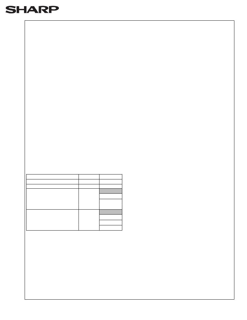
�Table� 5.� Identifier� Codes�
�Code� Address�
�Data�
�of� the� applied� V� PP� Voltage.� RP#� can� be� V� IH� or� V� HH� .�
�This� command� is� not� functional� during� block� erase� or�
�Manufacture� Code�
�00000�
�89�
�byte� write� suspend� modes.�
�Device� Code�
�Block� Lock� Configuration�
�00001�
�X0002� (1)�
�A6�
�4.5� Block� Erase� Command�
�?� Block� is� Unlocked�
�?� Block� is� Locked�
�?� Reserved� for� Future� Use�
�Master� Lock� Configuration�
�?� Device� is� Unlocked�
�?� Device� is� Locked�
�?� Reserved� for� Future� Use�
�00003�
�DQ� 0� =0�
�DQ� 0� =1�
�DQ� 1-7�
�DQ� 0� =0�
�DQ� 0� =1�
�DQ� 1-7�
�Erase� is� executed� one� block� at� a� time� and� initiated� by�
�a� two-cycle� command.� A� block� erase� setup� is� first�
�written,� followed� by� an� block� erase� confirm.� This�
�command� sequence� requires� appropriate� sequencing�
�and� an� address� within� the� block� to� be� erased� (erase�
�changes� all� block� data� to� FFH).� Block�
�preconditioning,� erase,� and� verify� are� handled�
�NOTE:�
�1.� X� selects� the� specific� block� lock� configuration�
�code� to� be� read.� See� Figure� 4� for� the� device�
�identifier� code� memory� map.�
�internally� by� the� WSM� (invisible� to� the� system).� After�
�the� two-cycle� block� erase� sequence� is� written,� the�
�device� automatically� outputs� status� register� data�
�when� read� (see� Figure� 5).� The� CPU� can� detect� block�
�erase� completion� by� analyzing� the� output� data� of� the�
�RY/BY#� pin� or� status� register� bit� SR.7.�
�Rev.� 1.3�
�发布紧急采购,3分钟左右您将得到回复。
相关PDF资料
LH28F160S3HNS-TV
IC FLASH 16MBIT 100NS 56SSOP
LH28F160S5HNS-S1
IC FLASH 16MBIT 70NS 56SSOP
LH28F320S3HNS-ZM
IC FLASH 32MBIT 110NS 56SSOP
LH28F320SKTD-ZR
IC FLASH 32MBIT 70NS 48TSOP
LHF00L28
IC FLASH 16MBIT 70NS 48TSOP
LPM409 CHASSIS
STNRD 4SLOT CHASSIS W/INPUT LEAD
LS15RB1201J04
POE SPLITTER 10.8W 12V @0.9A
LT1932ES6#TRMPBF
IC LED DRIVR WHITE BCKLGT TSOT-6
相关代理商/技术参数
LH28F008SCHT-TL12
制造商:未知厂家 制造商全称:未知厂家 功能描述:x8 Flash EEPROM
LH28F008SCHT-TL15
制造商:未知厂家 制造商全称:未知厂家 功能描述:x8 Flash EEPROM
LH28F008SCHT-V12
制造商:未知厂家 制造商全称:未知厂家 功能描述:x8 Flash EEPROM
LH28F008SCHT-V85
制造商:未知厂家 制造商全称:未知厂家 功能描述:x8 Flash EEPROM
LH28F008SCH-V
制造商:SHARP 制造商全称:Sharp Electrionic Components 功能描述:8-MBIT(1 MB x 8) SmartVoltage Flash MEMORY
LH28F008SCL-12
制造商:SHARP 制造商全称:Sharp Electrionic Components 功能描述:Flash Memory 8M (1M 】8)
LH28F008SCL-85
制造商:SHARP 制造商全称:Sharp Electrionic Components 功能描述:Flash Memory 8M (1M 】8)
LH28F008SCN-12
制造商:未知厂家 制造商全称:未知厂家 功能描述:x8 Flash EEPROM